Photovoltaic II: 182mm or 210mm, Which One?
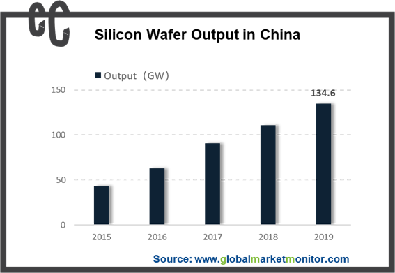
As of the end of 2019, the silicon wafer production of China was 134.6GW, a year-on-year increase of 25.7%, accounting for 98% of global production. In 2019, the total export volume of photovoltaic products of China was approximately US$20.78 billion, in which that of silicon wafers was US$2 billion, and the export volume was approximately 27.3GW. The global photovoltaic industry's dependence on China's production capacity has become more obvious.
At the same time, the competition among domestic silicon wafer manufacturers has not stopped for a moment. Nowadays, monocrystalline silicon dominates the market in terms of monocrystalline silicon and polycrystalline silicon. However, in terms of the size of silicon wafers, the market has not given an accurate answer.
Enquire before purchasing this report-
https://www.chinamarketmonitor.com/request.php?type=3&rid=228738
Size Battle
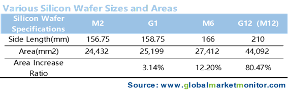
The battle over the size of silicon wafers began five years ago. In 2015, Longi and Zhonghuan teamed up to customize the M2 size standard, which is also the current mainstream size. The side length is 156.75mm, the diagonal length is 210mm, and the area of each wafer is 24432 square millimeters, and the market share is about 80%.
Since 2018, many players have released silicon wafers of different sizes such as 157mm, 158.75mm, and 161mm, and 163mm, and 166mm, and 180+mm, and 210mm.
In 2018, JinkoSolar launched the square monocrystalline silicon wafer G1 with a side length of 158.75mm, which is 3.14% larger than the M2 wafer.
Since then, M6 size product of Longi was released, with a side length of 166mm, a diagonal diameter of 223, and a silicon wafer area of 27412 square millimeters, which fully take care of the compatibility of the old capacity of silicon wafers, cells, and modules before 2019. It can be said that 166 is the best silicon wafer size for old production capacity and the easiest one to be widely promoted, as evidenced by the substantial increase in market share.
On August 16, 2019, Zhonghuan which applied semiconductor technology to the photovoltaic industry first launched M12 large-size silicon wafers with a side length of 210mm and the wafer area of 44,092 square millimeters, leading the photovoltaic industry to enter a new stage of large size.
Large-size silicon wafers are the best choice for the industry under the trend of reducing costs and increasing efficiency. However, due to the inconsistent size of silicon wafers used by enterprises, the manufacturing costs of auxiliary materials such as silicon wafers, cells to modules, and glass have risen sharply in the photovoltaic industry chain.
Therefore, for the 210 large-size silicon wafers launched by Zhonghuan, industry insiders express their opposition, because the current production of 210 has problems in hot spots, slicing losses, splits, brackets and inverter compatibility. The opponents believe that this is completely aside from the current situation.
Large Size Is the Certain Trend, But Who Is the Leader?
The reason why the size of silicon wafers has been increasing is that large-size silicon wafers reduce the cost of unit growth at the silicon wafer end, and dilute the non-silicon cost of a single watt in the cell, component, and system links, and the economic benefits are significant. Therefore, the development of large-size silicon wafers has become inevitable.
As using larger silicon wafers can further reduce costs, the two routes of 182mm and 210mm have not only sparked discussions among industry insiders, but also become a hot spot of public concern. The two camps of 182mm and 210mm silicon wafers expressed their opinions due to factors such as technology and becoming. Then we first understand the situation of the two, and then in-depth discussion will be more sensible.
The 182mm silicon wafer camp is mainly represented by including Longji, Jinkosolar, and other 5 companies, jointly advocating the establishment of a 182mm*182mm photovoltaic silicon wafer standard (M10) as the standard size of the research and development of next-generation silicon wafers, cells, and modules, which aims to avoid the inconsistency in the size of silicon wafers used by various companies, resulting in an increase in the manufacturing cost of auxiliary materials including silicon wafers, cells, modules, and glass in the photovoltaic industry chain, and to promote the establishment of a unified standard-based supply chain system for the entire industry.
182mm silicon wafers have taken care of the compatibility of silicon wafers, batteries, and component production lines to a certain extent, and the ability to reduce costs and increase efficiency is stronger than that of 166 silicon wafers. For component companies, compared with 210, 182-size silicon wafers and batteries are easy to buy in the market.
210mm silicon wafers represented by Zhonghuan have the strongest ability to reduce costs and increase efficiency and are fully compatible with future photovoltaic technology. Whether it is N-type battery technology or superimposed with perovskite, the future will be 210 as the standard.
Indeed, with the current production conditions of 210 silicon wafers, many problems will be encountered in the actual production and transportation process. However, temporary obstacles will not become a constant constraint, and the investment in the 210 mm silicon wafer production does not have high risk, without being eliminated now. Moreover, the benefit of the large flux of 210-size silicon wafers is an irreversible historical trend. On the other hand, 182 silicon wafers, although compatible with the actual conditions of all links in the current industry chain, have to worry about the lack of competitiveness in one year, especially the investment in battery production capacity cannot be recovered within one year.
One Strives for The Present, And the Other Focuses on the Future
It can be said that one is striving for the present and the other one focusing on the future, and there is no difference between good and bad. Following the trend of history, they will eventually be absorbed by the times. Social progress will inevitably be accompanied by the replacement of technology. This is a normal phenomenon, but which technology should be promoted needs the market to choose, too much subjective will disrupt the original development track.
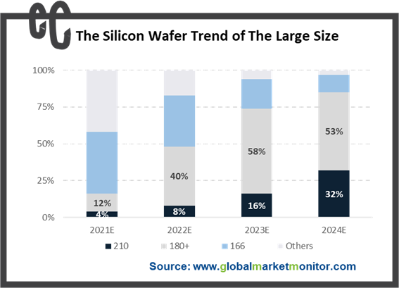
From the current form, 180+ silicon wafers suitable for the production conditions of each link of the current industrial chain are more easily accepted by the market, whose coverage will be wider than that of 210mm silicon wafers at an early stage. while with the advancement of technology, the bottleneck of the existing 210 wafer technology has been broken through, and large-scale production has been expanded. Then the market will give a new answer.
As the industry pioneer of 210mm silicon wafers field, Zhonghuan has obvious technical advantages. In the future, with the wide application of large silicon wafers, it will promote new development and innovation in the photovoltaic industry. At present, Zhonghuan's monocrystalline crystal production capacity in Hohhot has exceeded 30GW. After the completion of the next five-phase project construction, the production capacity will exceed 55GW. The five-phase project under construction will all have 210-size silicon wafer production capacity, which will greatly consolidate the company's leading position.
At the same time, as the 210mm silicon wafer field has less layout, industry companies will inevitably seize the first-mover position at the fastest speed. Especially companies that have no historical old production capacity and sufficient funds will inevitably accelerate their production speed, seize favorable terrain, and participate in early market segments. With the help of 210, Aiko Technology, Risheng Oriental, and Tongwei are expected to redistribute the market. Aiko Technology plans to complete 45GW of battery production capacity in 2022, occupying 20% of the global market share, and Risen Energy is not far behind, investing heavily in the 210mm module production line. Tongwei choose a 12-inch diameter equipment with 210mm without any hesitation.
LEARN MORE:
Silicon Wafers
https://www.chinamarketmonitor.com/reports/228738-solar-silicon-wafer-market-report.html
Solar Photovoltaic
https://www.chinamarketmonitor.com/reports/264709-solar-photovoltaic-materials-market-report.html
